Life after Trim: Using Factory Access Mode for Imaging SSD Drives
January 16th, 2019 by Oleg AfoninCategory: «Hardware», «Tips & Tricks»
Many thanks to Roman Morozov, ACELab technical support specialist, for sharing his extensive knowledge and expertise and for all the time he spent ditching bugs in this article.
SSDs are weird. They are weird in the way they write data, and even weirder in the way they delete information. In the good old days of striped magnetic recording, one could delete a file and rest assured its content was still there until overwritten at some (hopefully distant) moment in the future; not so on an SSD.
SSDs are different. They are different in handling deleted data, wiping evidence irreversibly in the background like they were criminals’ best friends. Just power on the SSD, and it’ll start background garbage collection, erasing trimmed blocks even if you connected it through a write blocker. Image the SSD, and you won’t find anything in the “empty” areas – even if the actual data was still there at the time of the imaging. One more thing: your SSD has more storage capacity than it says on the box. 5 to 15% of the physical storage capacity is dedicated for a non-addressable pool; any data one deletes from the SSD that is subsequently trimmed by the OS can go straight into that pool, without any chance of accessing or even addressing the blocks.
Until very recently your only way of accessing deleted evidence on an SSD would be taking the chips off and performing a labour-intensive, time-consuming (let alone extremely expensive) chip-off analysis. We asked our partners from a forensic data recovery lab, and they told us they can do a four-chip SSD in a matter of two weeks. They also said they’d rather steer clear of the recent ten-chip SSDs, and they won’t do anything about encryption.
Did I say encryption? It could be easier than you think. A recent discovery points out that Windows built-in BitLocker protection tends to delegate the job of encrypting data to the SSD controller (as opposed to doing the encryption on the computer using the CPU). As found in the research, many consumer-grade SSDs take it easy, keeping the encryption key unprotected in the storage chips on the SSD.
In this article, we’ll talk about a recent development in SSD forensics allowing to prevent background trimming of evidence and providing access to the entire storage capacity of the disk including non-addressable areas. This method employs a so-called factory access mode. However, before we talk about factory access mode, let us first have a look at how SSDs store information and why it is so easy to destroy evidence and so insanely difficult to recover it.
How SSDs Store Information
Unlike magnetic hard drives using more or less sequential writing (bar fragmentation and bad sector remapping), SSD drives ditch linear writing. Instead, information is broken into small blocks that are written to the different NAND chips concurrently. This parallel writing is the reason why SSDs are this fast; in a way, we’re talking about a RAID 0 (stripe) class array built with NAND chips installed on a single PCB.
What if you’ve got the cheapest and slowest SSD drive with only one NAND chip? Even this SSD will hardly ever write information in linear fashion (with possible exception of a brand-new, never written to SSD). Each physical block in the memory chip is dynamically assigned a logical address to help SSD controller do wear levelling. As a result, reading the content of a NAND chip will return a puzzle with information mixed broken into chunks that are mixed in what seems like a random fashion.
The SSD (and most other types of solid-state media) must translate NAND addresses in order to map out bad blocks and to provide wear levelling. Each NAND sell has a limited lifespan. Manufacturers rate their SSD drives for about 1000 to 1500 write cycles. Factors such as write amplification (another SSD specialty) negatively affect SSD lifespan, while smart SLC caching algorithms reduce cells’ physical wear even if the number of write operations is greater than that without caching. We’ll look at these and many other factors affecting SSD lifespan in our next article.
What really matter is that recovering just one single file could be extremely difficult without the help of the SSD controller. The expert will first have to reconstruct the translation table to figure out which NAND chips and at what exact addresses keep information. Different SSD controllers employ different formats for such translation tables; the more NAND chips the SSD drive contains, the more difficult it will be to reconstruct the translation table.
All Cells Are Equal, but Some Cells Are More Equal Than Others
The cost of electronic devices falls year over year. We’re used to that to the point we aren’t even noticing. SSD drives with storage capacities exceeding one or even two terabytes of data are now within reach of an average consumer, which was not the case just three years ago.
In order to produce solid-state storage with larger capacities at a lower price point, manufacturers have to squeeze more cells onto the same (or smaller) dye. This reduces the size of each cell, which negatively affects their rated lifespan (the number of write operations a cell can sustain without leaking charge). Alternatively (or, rather, in parallel) manufacturers invented a way to store more information in a single cell. While SLC-based NAND flash could keep one bit of information in every cell, MLC NAND stores two bits of data. Today’s SSD drives are mostly TLC (three bits of data per cell), while the cheapest drives may pack four bits per cell (QLC NAND). Each iteration makes NAND flash significantly slower and, more importantly, less reliable compared to lower density NAND:

As one can see, TLC cells are the slowest and least reliable. In order to speed up TLC-based SSD drives (and to improve their longevity), many manufacturers dynamically allocate some part of the storage as dedicated SLC cache. Blocks that are used as SLC cache require lower current to place that one bit of information. They wear less, and they are written to faster than TLC cells. The controller maintains the list of blocks that are used as SLC cache. If we attempt to read these blocks by accessing the chip directly while expecting three bits of data, these pseudo-SLC cells will return meaningless information.
Encryption
Most mid-range and all top of the line SSD drives offer one or several methods of hardware encryption. Some enterprise-grade SSDs encrypt information by default without the user even knowing. In such cases, the encryption key is stored open, so that the controller can read it off the NAND chip to decrypt data. If the user “encrypts” such a disk, it is just the small disk encryption key that gets encrypted.
Even if the encryption key is stored unprotected, finding it without the help of the SSD controller is extremely difficult if at all possible.
In other words, we need the controller to do the job for us. We need it to cope with error correction, address translation and potentially encryption. However, simply connecting the SSD to a write blocker, powering it on and imaging the disk like we did before is probably not the best idea.
How SSDs Delete Data
We figured that NAND cells sustain a limited number of write operations, which calls for advanced wear leveling algorithms. However, in addition to the limited lifespan, NAND cells have yet another property: a non-empty cell must be erased before you can write new data. NAND flash delivers fast reads, slow writes and very slow erases. So if you want to re-write a cell that already contains data, you must first erase the cell, and only then it can accept new data. While erasing NAND cells is already a very slow operation, you cannot simply wipe one or two cells. Instead, you’ll have to deal with pages and blocks.
So what is a cell, and why do we have to use pages and blocks? Let’s figure out the terms first. A cell is a basic unit for storing information. Depending on the type of flash memory (SLC, MLC, TLC or QLC) and depending on the mode of operation (e.g. SLC cache in MLC, TLC and QLC drives), a single cell can record one bit of data (SLC), two bits of data (MLC), three bits (TLC) or four bits (QLC). As an example, a Crucial MX550 SSD equipped with 3D TLC NAND can store 3 bits of data in each of its cells except when some parts of its storage pool operate in SLC mode as dynamic write acceleration cache. Writing to TLC cells in SLC mode is not only faster but puts significantly less stress on the cell, so the overall lifespan of the SSD can be improved along with write speeds.
Which brings us to another question. Can we read or write data from or to a single cell? You can’t.
Historically, rotating storage media such as traditional hard drives offered 512-bit sectors as a smallest data unit you could read or write. File systems such as FAT or NTFS read and write data in sectors, too. Things have changed once solid-state storage was introduced. NAND flash does not use sectors. Instead, it operates with pages and blocks.
A page is the smallest piece of data you can read off an SSD. Usually, an SSD drive can read one page per clock cycle. A single page contains a certain number of physical bytes (e.g. 528, 2112, 4320, 8640, 9216, 18592 bytes and so on). If you only need one byte of data, the SSD will read the entire page.
Each page can store 512, 2048, 4096, 8192, or 16534 bytes of data. As you can see, the amount of data a page can store is different from the number of physical bytes. The extra bytes are used for markers and ECC correction codes for every page. If we compare two SSD drives with pages containing 8192 bytes of data, we may discover that SSD1 uses 8640 physical bytes per page while SSD2 has 9216 physical bytes per page. The difference between these two SSDs would be solely in how much ECC correction each drive has.
Okay, we’re now content with cells and pages. Why do we need yet another entity? The thing is, while you can read a single page of data, you can only write (or erase) a certain number of pages at once. The minimum unit for writing (erasing) data is called a block. A single block contains a number of pages; in fact, it’s usually a whole lot of pages. A typical SSD operates with blocks comprised of 64, 128, 256 or even 512 pages. This is a huge amount of data to erase/write every time you change a single bit of data!
The number of write operations that can be sustained by NAND flash is limited (and quite small), so the SSD controller will do its best to minimize re-use of the blocks that have been already written to. This is what a simple SSD (without SLC cache) would do if you changed just 1 bit of data.
- The controller will read a block of data from NAND flash into RAM.
- The NAND block is marked to be erased (depending on the SSD and controller, it may be erased later on in background).
- The controller now makes the requested change in the data block stored in RAM.
- Finally, the modified block will be written to NAND flash. A different set of physical cells will be used to write new data for the purpose of wear levelling and write speed (since erase operations are much slower than writes).
When writing data, the SSD controller will try to choose blocks with the least rewrite count. In real life this means that the controller will write the same set of data to a different block. To make things look consistent for the OS, the controller will remap the block’s logical address on the fly. The “new” block will be assigned a certain address, while the “old” block will be either moved to the reserve pool in overprovisioned area or assigned a different address. The SSD will then erase the content of that block and increment its Erase Count parameter.
Reserve Pool and Overprovisioned Area
The SSD’s physical capacity is always higher than its advertised (and available) storage. While most modern SSD drives reserve 5 to 10 per cent of their storage capacity, some models have significantly higher percentage of their storage capacities that is unused. As an example, Crucial offers entry-level BX series SSD drives with 480 GB of storage, while their higher priced MX series advertise capacities of 500 GB. Both models are likely using 512 GB internal capacity (not accounting for ECC codes and markers, which makes physical capacity even higher). Since today’s NAND chips are manufactured in arbitrary sizes that are not necessarily a multiple of two, the real size of the chip can be e.g. 8.7 GB instead of exactly 8.
The difference is due to the size of so-called reserved area otherwise known as overprovisioned area. The extra blocks are used for wear leveling and swap pool, allowing the SSD controller to quickly pick an empty block when it needs to rewrite some data.
It is important to note that overprovisioned blocks may contain data. Once the SSD controller pushes a data block into a non-addressable pool, the block is marked as empty (“trimmed”). The trimmed blocks will be queued for garbage collection, which works as a background process. The garbage collection process will actually clean the content of trimmed data blocks. The process is not instant; it may take a while to complete depending on the number of data blocks being trimmed, the type and speed of the NAND flash. Some SSD drives may take up to 15 minutes to finish cleaning up trimmed blocks. We’ve also seen SSD drives that never actually cleaned the content of overprovisioned blocks due to firmware bugs (this, in particular, is the reason why most military data sanitization standards demand physical destruction of solid-state storage media as opposed to relying on any software methods).
SSD Drives Wipe Evidence
Another very important note is the fact one cannot easily stop an SSD drive from completing the background wipe cycle. Once a range of data blocks is trimmed (a nearly instant operation), even if the SSD drive is disconnected immediately, the garbage collection process will resume its work the moment the SSD drive is powered on. SATA write blocking devices do not affect this process and cannot be used to prevent background garbage collection.
What happens if one attempts to read a trimmed block that still contains data? The result depends on a particular implementation of Read After Trim. There are four distinct modes of reading information from trimmed blocks:
- Non-deterministic Trim: undefined. When reading a trimmed block, the SSD controller may return the actual data, all zeroes or something else. Interestingly, the result may differ between read attempts (SATA Word 169 bit 0). This more is rarely used by reputable SSD makers; however, discount bin SSD drives may still have it.
- Deterministic Read After Trim (DRAT): the SSD controller will always return a pre-defined value when reading trimmed blocks regardless of their actual content. The value could be all zeroes, but it could also be something else (SATA Word 69 bit 14). This is the most common method used in consumer SSD drives.
- Deterministic Zeroes After Trim (DZAT): all trimmed blocks will instantly read as zeroes regardless of their actual content (SATA Word 69 bit 5). This mode is commonly used in enterprise-level SSD drives. Most NAS manufacturers require this mode if one wants to make an SSD RAID.
Users can easily determine which mode their SSD drive operates by running the following command: hdparm –I.
Example:
$ sudo hdparm -I /dev/sda | grep -i trim
* Data Set Management TRIM supported (limit 1 block)
* Deterministic read data after TRIM
Practically speaking, DRAT and DZAT effectively prevent access to real data immediately after the Trim command has been issued. Even if the SSD drive is formatted with Quick Format, its entire content will instantly become inaccessible; a huge departure from behavior exhibited by non-encrypted magnetic hard drives. There would be no way to access trimmed data, and there would be no way to prevent background garbage collection destroying evidence still stored in trimmed blocks.
Life after Trim: SSD Factory Access Mode
Until very recently, forensic experts were forced to follow one of the two extraction strategies. Using the first strategy, experts would be treating SSD drives similar to magnetic hard drives, which would make deleted data inaccessible.
The other strategy (chip-off analysis) would require taking the NAND chips off PCM board and performing a lengthy, labor consuming analysis. Analyzing an SSD with just four chips could take up to two weeks, while 10-chip disks would be nearly impossible to process.
Sending an SSD drive to the manufacturer for data recovery was rare occurrence, yet technically speaking this would be the optimal strategy as manufacturers can go through SSD factory mode.
Solid-state storage media with built-in controllers (which includes SSD drives, USB flash drives, eMMC chips and even SD cards) have several modes of operation. By default, they work in the “standard” mode, in which one can read and write data, trim blocks or format partitions. However, all solid-state storage devices also have a special access mode sometimes called “factory access mode” or simply “factory mode”. In this mode manufacturers initialize the controller, upload firmware, test NAND memory and build initial lists of remapped bad blocks. In factory access mode, manufacturers can access information stored in the NAND chips directly complete with all service information. Factory access mode is built in to every single SSD drive in existence including those assembled in underground factories from recycled parts.
In factory access mode, the SSD can execute low-level commands sent via the ATA interface (or USB, or PCI-E, or whatever other interface the SSD has). In factory mode, the SSD can perform a number of things it cannot do while in standard mode.
Factory access mode is there for a reason. In magnetic hard drives, factory access mode is used for low-level diagnostics, allowing manufacturers reveal manufacturing defects (e.g. magnetic head defects) early on. In solid-state media, factory mode is used to detect bit errors in NAND cells. It is also used by many manufacturers to provide data recovery services when customers send the disk in. Finally, factory access mode is used to upload firmware and to create service areas such as the address mapping tables when initializing the disk.
Which Manufacturers Use Factory Access Mode?
Factory access mode is used by absolutely every SSD manufacturer. In fact, manufacturers of USB flash drives, eMMC chips, SD cards and other types of “smart” storage media equipped with microcontrollers all use factory access mode to program, test and initialize storage devices. Even manufacturers assembling their disks from off the shelf parts (such as the popular Phison PS2251-07 controller) have access to factory mode. Factory access mode is built into all SATA, NVME, USB and other SSD drives.
Features of Factory Access Mode
Factory access mode opens a number of possibilities that aren’t available to ordinary users. The following features are of particular interest to forensic specialists:
- Reading raw data from physical data blocks. The blocks are return in the true sense of “raw”, complete with encoding and ECC data correction information. This is the closest one can get to chip-off without actually pulling the chips. Note that encrypted data will not be decrypted in this mode even if the media encryption key (MEK) is not encrypted.
- Reading a logical data block. This includes the necessary decoding operations including deMIXing pages and blocks, converting encoded pages and performing ECC corrections. In addition, SSD drives featuring hardware encryption will decrypt encrypted data (if default media encryption key is used). In other words, this is the easiest way to read data off an SSD including trimmed and overprovisioned blocks.
- For encrypted SSD drives: look up for the module containing the media encryption key (MEK). While SSD encryption is beyond the scope of this article, it is important to note that certain encryption methods (such as the Windows 10 version of BitLocker) makes use of SSD built-in encryption features as opposed to encrypting data using the CPU. As a result, an expert may be able to locate the BitLocker encryption key and decrypt the data without running a lengthy attack.
- Access blocks in the overprovisioned area as well as blocks outside of the addressable pool defined by the translation table (Remapped, Relocated and Reserved blocks).
- Accessing SMART records.
- Accessing (lookup and read) system areas containing SSD firmware and translation tables.
- Reading system areas and saving them for subsequent analysis.
- Booting the SSD into a different firmware by placing the microprogram into the controller’s RAM; using a different (rebuilt) translation table (e.g. if the original translation table is damaged or unreadable).
For digital forensic experts, two additional features can be of particular interest. First, one can temporarily disable controller’s background processes such as garbage collection, wear leveling and address remapping. This effectively prevents SSDs from destroying evidence in background. Second, one can access data stored in non-addressable blocks (overprovisioned area, reserve pool etc.) This enables access to recently deleted data.
Solid-state drives rely on the Trim command to improve writing performance by pre-emptively erasing blocks that are no longer used to hold meaningful data. When a file is deleted or if disk space becomes available in a different way (e.g. the disk is formatted), the Trim command allows the SSD controller to release unused blocks. Released blocks are scheduled to be processed by the built-in garbage collector; they can be also remapped (assigned a different physical address or pushed outside of the addressable space into the overprovisioned area). Importantly, the Trim command itself does not erase data; it’s garbage collection process that does.
Released data blocks can retain their original data for a certain period of time. The amount of time these blocks will retain the original data depends on multiple factors ranging from SSD’s current load to the model of SSD controller, its firmware and the variable priorities set by the manufacturer for a particular model. Background garbage collection is resource consuming. SSDs prioritizing garbage collection over read/write operations exhibit a temporary reduction of I/O performance. On the other hand, SSDs prioritizing current I/O over garbage collection exhibit long delays between the time the block has been trimmed and the time it’s being actually erased. This variety can make it possible to extract information from trimmed/overprovisioned blocks long after they have been released.
Using Factory Access Mode to Extract Data
Factory access mode can and should be used for forensic imaging of solid-state media. This is the only mode forensic experts can use to extract information from SSD drives without the risk of losing evidence due to background wiping, and this is the only mode allowing access to non-addressable, overprovisioned blocks. Using factory access mode is orders of magnitude easier (and substantially less expensive) compared to the chip-off process, especially if one is imaging an encrypted device.
Importantly, there are no established standards for accessing information in factory mode; there is no universal method of switching a given SSD drive into factory access mode, and there is no standard set of commands available in factory mode for all models and manufacturers. Factory access mode is barely (if ever) documented. In many cases, factory access mode is only available to the larger authorized service centers of each respective manufacturers.
It is common for the forensic community to rely on non-OEM third-party tools for performing extractions, and SSD imaging is no exception. ACELab PC-3000 SSD Suite enables low-level SSD imaging through factory access mode for a wide range of storage devices. The toolkit can image healthy and damaged SSD drives even if they are unbootable or throw out an error message. Due to the sheer variety of OEMs, models of SSD controllers and firmware versions, we leave the details to ACELab; one can start reading from the following three articles:
- PC-3000 SSD. Active Utilities (Main concept description)
- PC-3000 SSD. Silicon Motion (SM) Utility
- PC-3000 SSD. Phison Utility for PS3109, PS3105, PS3108, PS3109, PS3110, PS3111, TC58NC1000, TC58NC10100
Generally speaking, SSD imaging via factory access mode requires the following steps.
- Prevent SSD controller from booting into “standard” mode by blocking controller’s access to NAND flash chips. This prevents the controller from loading firmware and ensures that no background process can destroy evidence.
- Switch the SSD drive to factory access mode.
- Read SSD firmware and system areas. If necessary, reconstruct damaged translation tables.
- Upload microcode into the SSD controller RAM. Upload translation tables and other system data.
- Boot SSD controller to the code in RAM.
- Use factory access modes to access information on the SSD drive.
Each SSD drive (or, rather, each SSD controller) employs a different sequence for switching into factory mode. Before the SSD drive can be switched to factory access mode (otherwise known as Factory Mode, Safe Mode, Recovery Mode etc.), one must first ensure that the SSD controller does not boot in Standard mode when powered on. This can be achieved by blocking access to NAND flash chips that contain SSD firmware and system areas. One can block access to NAND chips by shorting service pins on the PCB.
Blocking access to NAND chips can also help starting a damaged SSD drive with corrupted translation tables. If the translation table is corrupted, the SSD may enter a bootloop “load microcode > error > reset > load microcode > error …” If the SSD is damaged and is in a bootloop, it will not accept the service command to switch into factory access mode due to 100% load (as reported by the always active BSY-state ATA command).
This is how you block access to NAND chips on a Crucial BX100:

Next, we’ll connect the SSD to ACELab PC-3000 in order to switch it into factory access mode. Factory access mode is activated by sending a service command (widely different per OEM/controller) to the SSD controller. Then, we’ll upload the LDR code into the controller’s RAM.
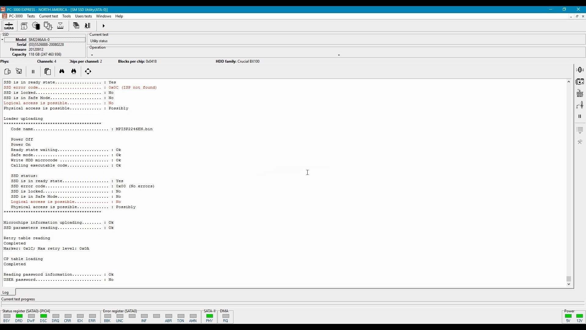
If we were able to successfully upload microcode, the next step will be reading/recovering the translation table. Damaged translation tables can be automatically or manually reassembled.
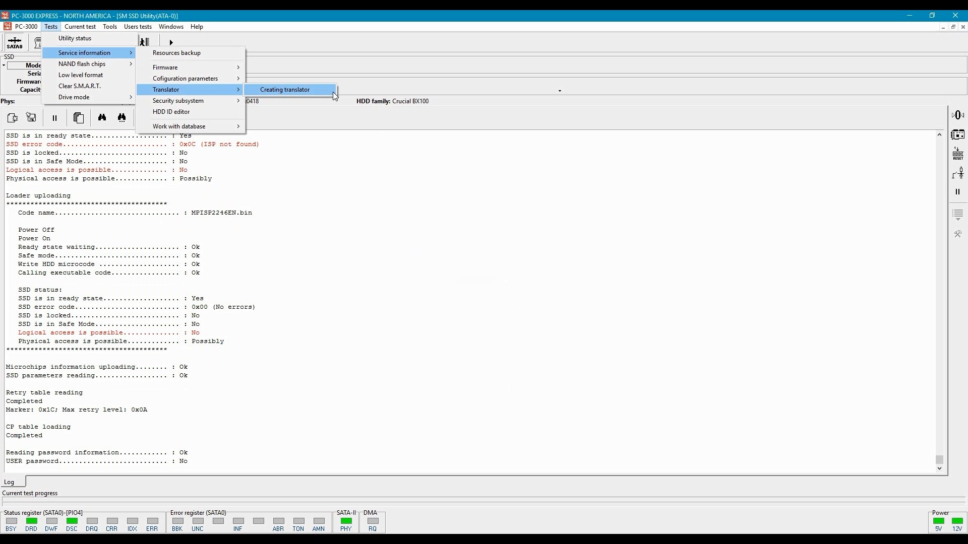
Translation tables must be uploaded into RAM of the SSD controller:

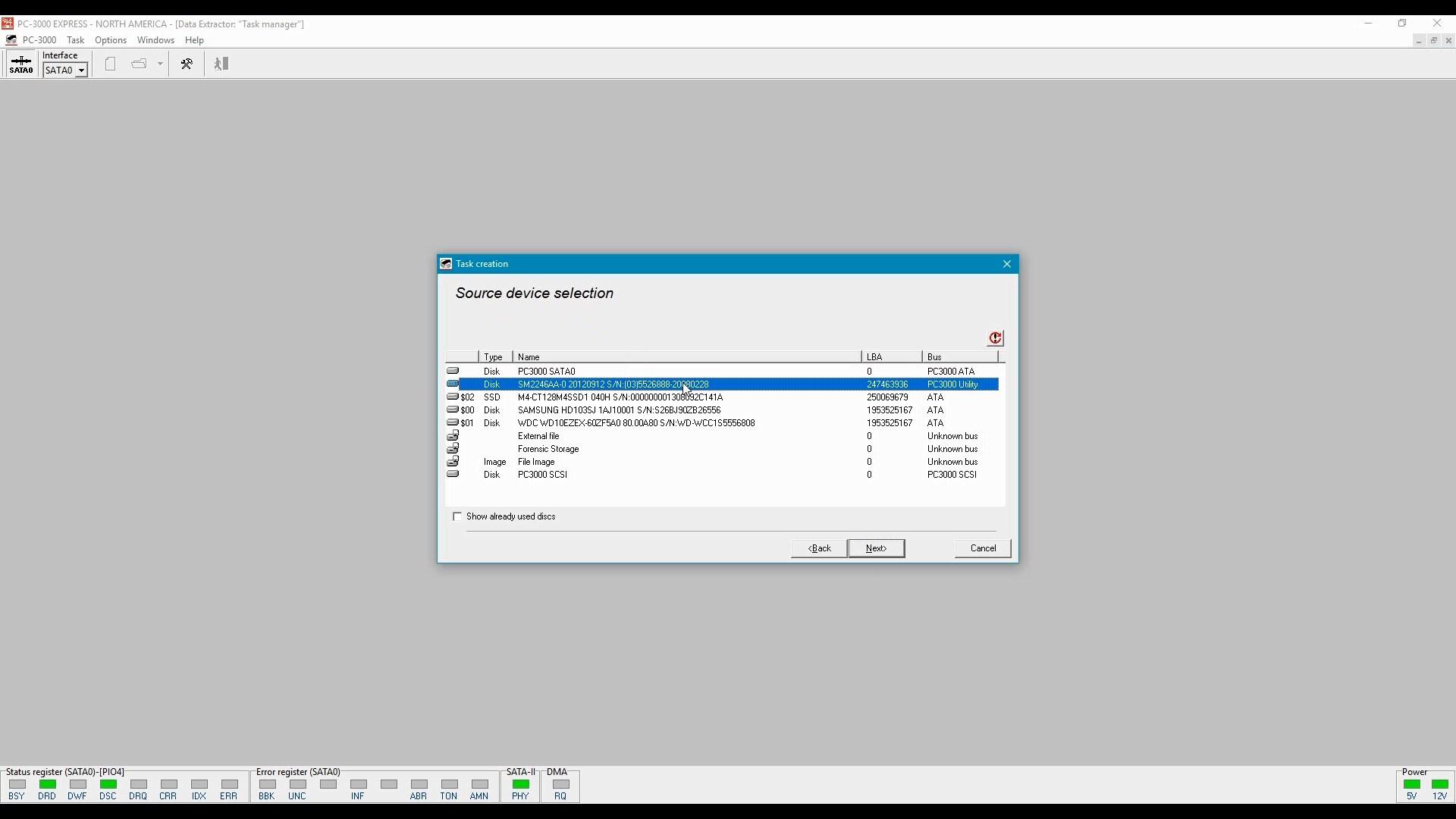
Then one can use the Data Extractor app to image the SSD drive. The data will be saved as standard disk image. You will be able to read blocks that have been trimmed but not yet physically erased.
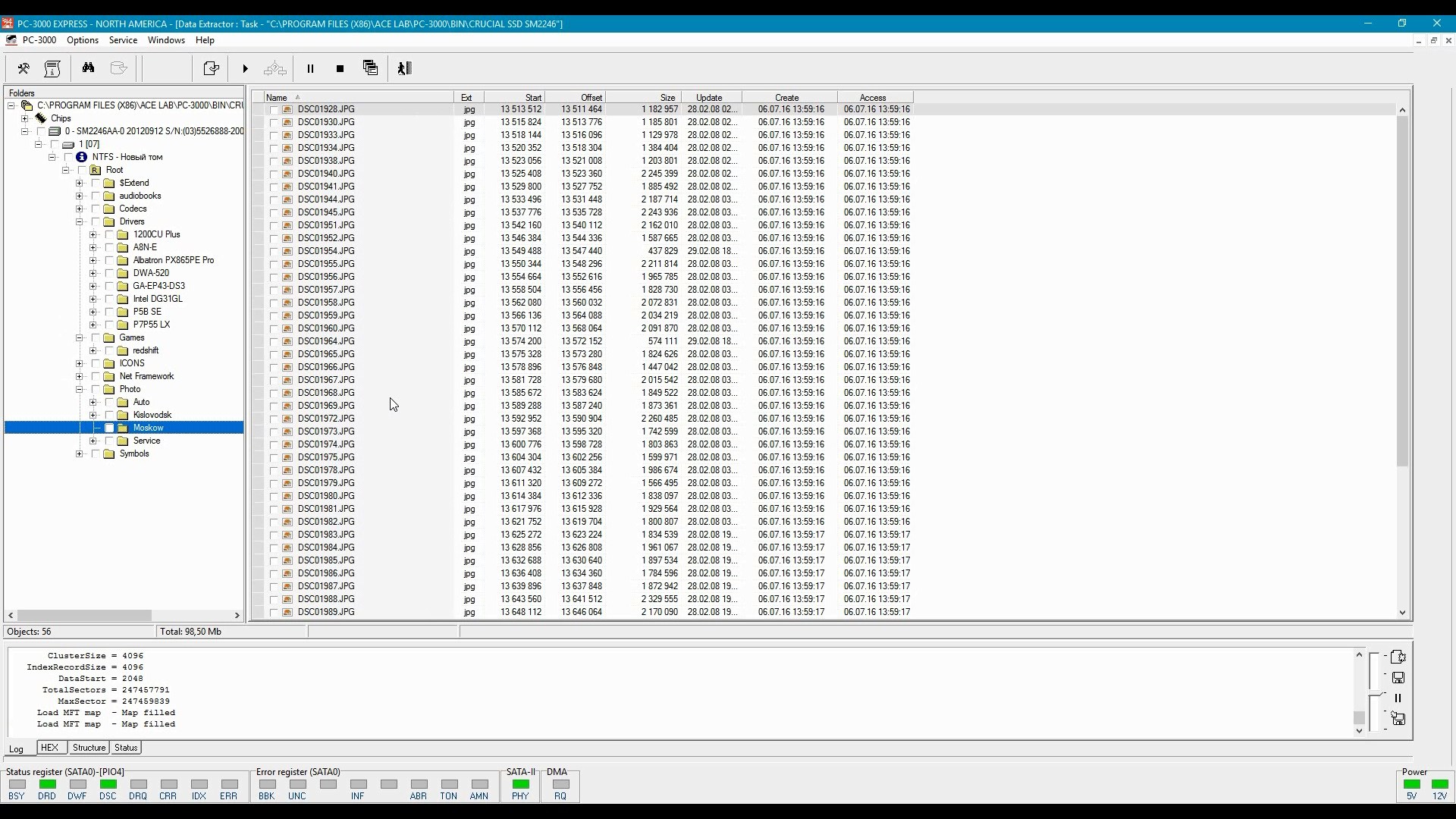
For faster/easier analysis, one can extract the content of the disk as a file system. In this mode, only existing files will be saved; deleted data will not be available.
Conclusion
SSD forensics is an ongoing subject. While SSD manufacturers increase storage densities and implement non-trivial methods for wear leveling, caching and write acceleration, forensic experts start using new methods for imaging solid-state media. In this article, we discussed the possibility of using factory access mode for imaging SSD drives.


- Elcomsoft Phone Viewer 5.50 packs multiple compatibility improvements19 March, 2024
- Bootloader-level extraction for 16.7.6 and 15.8.215 March, 2024
- Elcomsoft Distributed Password Recovery introduces resource management capabilities20 February, 2024
- Enhanced support for legacy devices1 February, 2024
- Supporting Sage 50 Accounting Canadian Edition17 January, 2024