Why SSDs Die a Sudden Death (and How to Deal with It)
January 18th, 2019 by Oleg AfoninCategory: «General», «Hardware», «Software»
Many thanks to Roman Morozov, ACELab technical support specialist, for sharing his extensive knowledge and expertise and for all the time he spent ditching bugs in this article.
In our previous article Life after Trim: Using Factory Access Mode for Imaging SSD Drives we only mentioned reliability of SSD drives briefly. As you may know, NAND flash memory can sustain a limited number of write operations. Manufacturers of today’s consumer SSD drives usually guarantee about 150 to 1200 write cycles before the warranty runs out. This can lead to the conclusion that a NAND flash cell can sustain up to 1200 write cycles, and that an SSD drive can actually survive more than a thousand complete rewrites regardless of other conditions. This, however, is not fully correct. Certain usage conditions and certain types of load can wear SSD drives significantly faster compared to their declared endurance. In this article, we’ll look why a perfectly healthy SSD drive with 98-99% remaining life can die a sudden death. We’ll also give recommendations on tools and approaches that can get the data back even if the SSD drive is corrupted or does not appear in the system.
NAND Flash Endurance: Expectations vs. Reality
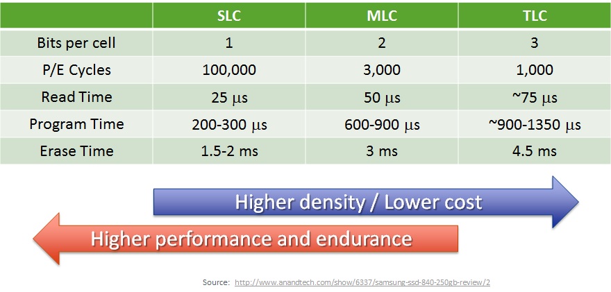
Major SSD manufacturers such as Crucial and Samsung are offering 5-year limited warranties to their recent models. The manufacturers specify the maximum amount of data that can be written to an SSD drive during the warranty period.
For example, this is what Crucial and Samsung promise for their recent SSD series.
| Endurance Rating | 2TB | 1TB | 500GB | 250GB |
| Crucial MX500 (3D TLC) – TBW (Terabytes Written) | 700TB | 360TB | 180TB | 100TB |
| Samsung 860 EVO (3D TLC) – TBW (Terabytes Written) | 1200TB | 600TB | 300TB | 150TB |
| Samsung 860 PRO (3D MLC) – TBW (Terabytes Written) | 2400TB | 1200TB | 600TB | 300TB |
Independent researchers appear to confirm manufacturers’ stated endurance ratings. This TechReport test is fairly old, but their findings are consistent with the recent ongoing tests by 3DNews.ru. “All of the drives surpassed their official endurance specifications by writing hundreds of terabytes without issue. Delivering on the manufacturer-guaranteed write tolerance wouldn’t normally be cause for celebration, but the scale makes this achievement important”, concluded TechReport’s Geoff Gasior. Long-term testing of multiple SSD models performed by 3DNews suggests that even mid-range SSD drives can be overwritten many thousand times before their flash memory starts showing signs of degradation. This, however, does not explain why some users have their SSD drives fail well within their warranty periods after overwriting the SSD just 20 to 30 times (with 98-99% of the rated lifespan still remaining).
The thing is, today’s TLC flash cannot sustain thousands of write cycles without significant degradation. In fact, a typical cell can sustain 20 to 50 write/erase cycles before it starts leaking charge. Low-quality NAND flash can be less robust, while SLC caching can improve the number of write cycles, yet the end result is the same: a NAND cell becomes less reliable in retaining electrons.
So how do these numbers relate to manufacturers’ declared endurance of more than 1000 write cycles, and how reliable are those SSD drives after all? Let’s try to find out.
Speaking of wear, each write operation slightly damages a NAND cell. Writing a single bit of data in SLC mode requires lower voltage compared to writing multiple bits of data in MLC or TLC mode. As a result, MLC or TLC based SSD drives equipped with SLC cache can sustain significantly higher load (especially random writes) compared to lower-cost counterparts that don’t have SLC cache. In some scenarios involving frequent writes of small chunks of data, the use of SLC cache can boost SSD’s real endurance up to 100 times compared to SSD drives without SLC cache:
After a certain number of program/erase cycles, NAND cells can no longer retain charge and start leaking electrons. One can still write data in worn out cells; the data can be read back successfully immediately after write. However, the cells will leak charge, and will only retain data for some very limited time.
Let us do an imaginary test and write “1 0 0” into a TLC cell. Immediately after writing, we could read the cell successfully; the charge would still correspond to “1 0 0”. We power off the SSD drive and let it sit for two days, then power it back on and read the cell. The charge is still “1 0 0”. Let’s power it off again, this time for two weeks. After reading the cell in two weeks’ time, the charge is now at a “0 1 0” level. Two more weeks, and the charge is “0 0 1”, followed by “0 0 0” in two more weeks.
The time a NAND cell can retain charge after a certain number of programming cycles is a major criteria when calculating the endurance rating. Most NAND flash manufacturers specify that cells must retain charge for at least two weeks at high temperatures (e.g. in data center environment). This time is significantly longer at home temperatures. During the specified retention period some cells are allowed to leak charge, but such bit errors must be correctable via ECC.
Two weeks is scary; in real life, reputable manufacturers use NAND chips that significantly exceed the minimum specifications.
Image by The Truth about SSD Data Retention (c) AnandTech
What happens to NAND flash chips that do not pass SSD OEMs’ stringent requirements? There is never lack of demand for low-cost sub-standard NAND chips. Third-tier manufacturers such as Kingspec, Smartbuy or Silicon Power purchase such inexpensive chips in bulk, producing low-cost SSD drives with varying reliability. Alternatively, manufacturers can still use sub-standard NAND chips in their SSDs by boosting the number of reserved blocks (and selling SSD units with lower advertised capacity, e.g. 480 GB as opposed to 500 GB). Yet another alternative (mainly employed by Crucial/Micron) would be using sub-standard TLC chips in MLC mode, which significantly boosts reliability. A great example of the last two approaches combined is Crucial BX300, a 3D MLC drive with 480 GB advertised capacity.
High temperatures negatively affect the ability of NAND flash to retain charge. As the temperature increases, the electrons escape the floating gate faster. This cell loses charge, and the data becomes unreadable. ACELab performed a controlled test in an attempt to verify the effect of high temperatures on the ability of NAND cells to retain charge. The test was conducted on an old SLC chip, which was able to sustain the temperature of +480C. Heated beyond this temperature, the chip was physically damaged. Notably, today’s MLC and TLC chips started experiencing bit errors at significantly lower temperatures. For this reason, some experts prefer using heated wires to cut chips off the PCB instead of unsoldering.
While we only need 3.3V to read data, we must supply 12V to erase or program cells. The higher voltage is required to place electrons in the NAND cell. As higher voltages are applied, the insulating layer between cells starts degrading, allowing more electrons escape as the time passes. The thinner the isolation layer becomes, the faster it will start to degrade, and the less program/erase cycles a cell can sustain.
Samsung Evo 840, one of the early SSD drives based on planar TLC flash, was an excellent example. The manufacturer was overly optimistic when estimating lifespan of the then-new TLC flash cells. The cells degraded significantly faster than planned. Unable to withstand even the modest 20 to 30 program/erase cycles, the cells leaked charge in powered-off state extremely fast. Many users lost data from unpowered Evo 840 drives after only 30 days of storage. Samsung fixed the issue with a firmware update, which didn’t help correcting a hardware problem. The second fix added a background process that “refreshed” the content of affected NAND cells by periodically erasing/rewriting their content. Needless to say, the fix negatively affected real-life endurance of the drives, wearing cells much faster than planned. As a result, Samsung Evo 840 got a well-deserved reputation of the worst SSD drive in history.
Manufacturers learned their lesson and stopped using planar TLC memory in new models, switching to the much more robust 3D NAND instead. This is how 3D TLC NAND stacks against planar MLC and planar TLC types:
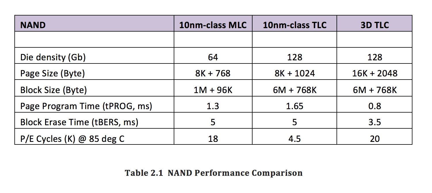
(Source: 3D TLC NAND To Beat MLC as Top Flash Storage EE|Times)
There are other technologies that are used to increase lifespan of the NAND cells. For example, many manufacturers dedicate part of the drive’s capacity as SLC cache. Writing data into a TLC cell in SLC more requires lower voltage, and has significantly smaller negative effect on the cell’s isolation layer. SLC cache is extremely effective if the SSD drive is used in environments with a frequent writes of small data blocks (e.g. databases). Constant firmware refinements allowed drastically reducing write amplification, which reduces the number of program/erase cycles required to store the same amounts of data.
Why SSD Drives Fail with no SMART Errors
SSD drives are designed to sustain multiple overwrites of its entire capacity. Manufacturers warrant their drives for hundreds or even thousands complete overwrites. The Total Bytes Written (TBE) parameter grows with each generation, yet we’ve seen multiple SSD drives fail significantly sooner than expected. We’ve seen SSD drives fail with as much as 99% of their rated lifespan remaining, with clean SMART attributes. This would be difficult to attribute to manufacturing defects or bad NAND flash as those typically account for around 2% of devices. Manufacturing defects aside, why can an SSD fail prematurely with clean SMART attributes?
Each SSD drive has a dedicated system area. The system area contains SSD firmware (the microcode to boot the controller) and system structures. The size of the system area is in the range of 4 to 12 GB. In this area, the SSD controller stores system structures called “modules”. Modules contain essential data such as translation tables, parts of microcode that deal with the media encryption key, SMART attributes and so on.
If you have read our previous article, you are aware of the fact that SSD drives actively remap addresses of logical blocks, pointing the same logical address to various physical NAND cells in order to level wear and boost write speeds. Unfortunately, in most (all?) SSD drives the physical location of the system area must remain constant. It cannot be remapped; wear leveling is not applicable to at least some modules in the system area. This in turn means that a constant flow of individual write operations, each modifying the content of the translation table, will write into the same physical NAND cells over and over again. This is exactly why we are not fully convinced by endurance tests such as those performed by 3DNews. Such tests rely on a stream of data being written onto the SSD drive in a constant flow, which loads the SSD drive in unrealistic manner. On the other side of the spectrum are users whose SSD drives are exposed to frequent small write operations (sometimes several hundred operations per second). In this mode, there is very little data actually written onto the SSD drive (and thus very modest TBW values). However, system areas are stressed severely being constantly overwritten.
Such usage scenarios will cause premature wear on the system area without any meaningful indication in any SMART parameters. As a result, a perfectly healthy SSD with 98-99% of remaining lifespan can suddenly disappear from the system. At this point, the SSD controller cannot perform successful ECC corrections of essential information stored in the system area. The SSD disappears from the computer’s BIOS or appears as empty/uninitialized/unformatted media.
If the SSD drive does not appear in the computer’s BIOS, it may mean its controller is in a bootloop. Internally, the following cyclic process occurs. The controller attempts to load microcode from NAND chips into the controller’s RAM; an error occurs; the controller retries; an error occurs; etc.
However, the most frequent point of failure are errors in the translation module that maps physical blocks to logical addresses. If this error occurs, the SSD will be recognized as a device in the computer’s BIOS. However, the user will be unable to access information; the SSD will appear as uninitialized (raw) media, or will advertise a significantly smaller storage capacity (e.g. 2MB instead of the real capacity of 960GB). At this point, it is impossible to recover data using any methods available at home (e.g. the many undelete/data recovery tools).
Data Recovery through Factory Access Mode
You can still attempt to recover information from a failed SSD drive if it does not appear in the system or is recognized as raw media. Do not try using data recovery tools you can download from the Internet; none of those can break the bootloop or activate the drive’s factory access mode. (In case you missed it, we have a comprehensive article explaining SSDs’ factory access mode: Life after Trim: Using Factory Access Mode for Imaging SSD Drives).
The only thing one can do other than sending the disk to the manufacturer is using the disk’s factory access mode. Factory access mode is built into all SSD drives, no exceptions. Large data recovery services and authorized service facilities of major manufacturers have tools that can activate factory access mode, rebuild corrupted translation tables and read information off the chips. Unfortunately, many small OEMs selling budget SSD drives built with off the shelf parts and using B-stock NAND chips do not have any repair facilities at all. For those manufacturers dumping the broken SSD drive and just mailing a replacement is far easier than building and maintaining a repair facility. If this is the case, finding a reputable independent data recovery service will be the only way to access information.


- Elcomsoft Phone Breaker 11.03: universal binary for Macs, SMS two-factor authentication restored16 July, 2026
- iOS Forensic Toolkit 10.10 adds pairing-free sideloading of the extraction agent24 June, 2026
- Elcomsoft Phone Breaker 11.2: downloads iOS 26 iCloud backups18 June, 2026
- Elcomsoft Phone Breaker 11.1: reliable iCloud backup extraction26 May, 2026
- ElcomSoft Phone Breaker 11: full overhaul of iCloud extraction30 April, 2026